Transistor symbol
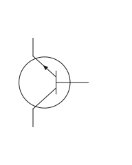
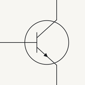
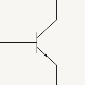
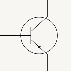
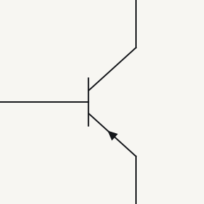
In a bipolar (BJT) symbol the arrow is always on the emitter (E): pointing out means NPN, in means PNP. The base (B) meets the flat bar; the other lead is the collector (C). The MOSFETs drawn here carry their arrow on the body instead.Source 1Source 2Source 3Source 4
Symbol and what it is doing
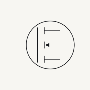
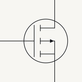
US style
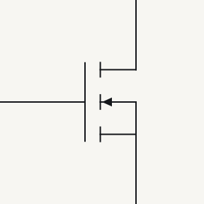
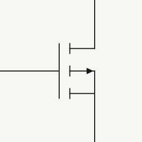
IEC style
Turn the base drive on and off. The printed transistor stays the same; the highlight shows when the switch model treats the collector–emitter path as conducting.
C–E open. Under the BJT switch model, no base drive gives cutoff: the collector–emitter path is treated as open.
C–E conducts. Under the BJT switch model, sufficient base drive for the connected load gives saturation: the collector–emitter path conducts.
Terminals
Parts of the drawing
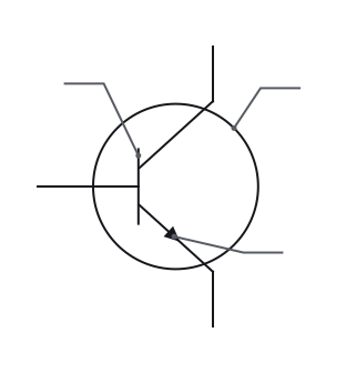
- 1 Flat bar
- As in the terminal key.
- 2 Enclosing circle
- The enclosing circle may be omitted from a transistor symbol. With the same internal marks and terminal connections, either drawing represents the same transistor.Source 6
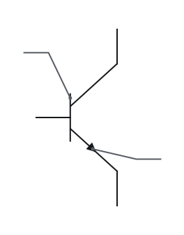
- 1 Flat bar
- As in the terminal key.
-
0°
-
90°
-
180°
-
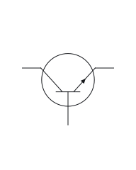
270°
-
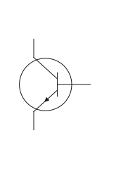
Mirrored
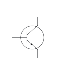
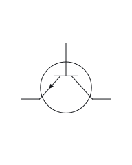
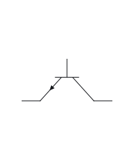
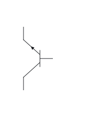
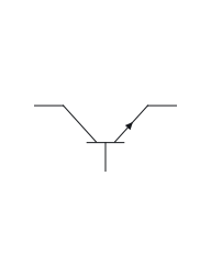
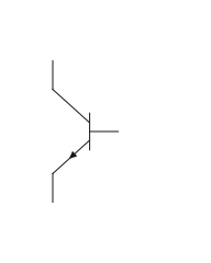
Rotating or mirroring a whole symbol, with its terminal identities and connections preserved, does not change the component. The terminal labels move with the drawing.Source 9
-
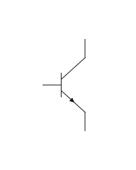
0°
-
90°
-
180°
-
270°
-
Mirrored
Rotating or mirroring a whole symbol, with its terminal identities and connections preserved, does not change the component. The terminal labels move with the drawing.Source 9
Variants
- BCEBCE
PNP transistor
As in the terminal key (E).
- GDSGDS
N-channel MOSFET
A MOSFET uses gate voltage relative to source to control its channel between drain and source. The three-terminal form shown here connects its body internally to source.Source 3
- G
- The gate is the insulated terminal drawn parallel to the channel with a gap between them.Source 3
- D
- The drain (D) is the other channel terminal: the channel runs between drain and source.Source 3
- S
- The source (S) is the channel terminal joined to the body in the three-terminal form shown here, so the controlling gate voltage is applied between gate and source.Source 3
- GDSGDS
P-channel MOSFET
In the body-arrow MOSFET convention used here, the arrow points toward the channel for N-channel and away for P-channel. Other MOSFET symbol forms place the arrow differently.Source 2Source 3
Telling them apart
- A MOSFET's gate is drawn beside the channel with a gap between them, and its arrow sits on the body. A bipolar transistor's base lead meets its bar directly, and its arrow sits on the angled emitter lead.Source 2Source 3Source 4
- In a PNP transistor symbol the emitter arrow points in, toward the base; that inward arrow is the only mark that tells it from an NPN symbol.Source 4Source 8
- The N in a device's name does not fix which way its arrow points. Each junction arrow points toward the N-type side: an NPN transistor's emitter arrow points out, but an N-channel MOSFET's body arrow points in, toward the channel.Source 2Source 3Source 4
- In a P-channel MOSFET symbol the body arrow points out, away from the channel, because the arrow points toward the N-type body.Source 2Source 3
Which way the arrow points
-
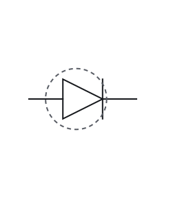
Diode
Points from anode to cathode
-
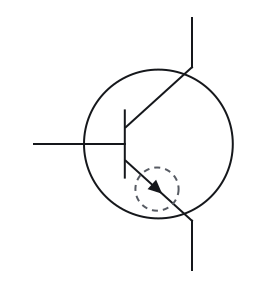
NPN transistor
Points out of an NPN transistor
-
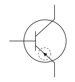
PNP transistor
Points in, toward the base
-
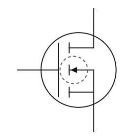
N-channel MOSFET
Points in, toward the channel
-
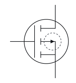
P-channel MOSFET
Points out, away from the channel
-
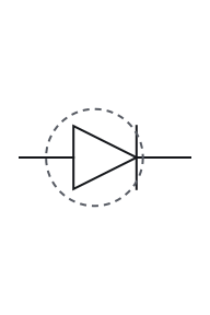
Diode
Points from anode to cathode
-
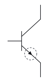
NPN transistor
Points out of an NPN transistor
-
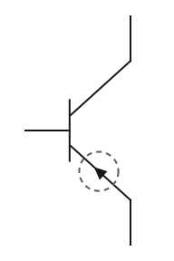
PNP transistor
Points in, toward the base
-
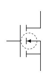
N-channel MOSFET
Points in, toward the channel
-
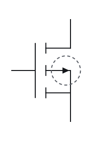
P-channel MOSFET
Points out, away from the channel
Notes
A bipolar transistor is steered at its base
A bipolar transistor has base, collector and emitter terminals. In the current-controlled model used here, base drive controls conduction between collector and emitter.Source 1 Its emitter arrow is read the same way as the triangle in a diode symbol, in the direction of conventional current.
B, C and E name roles, not pin positions
A schematic symbol shows how terminals connect, not where they are on a real part. Terminal letters such as E, B and C or A and K do not give lead order or package layout; the part's own documentation does.Source 9Source 13Source 14 The letters name what each terminal does: base drive controls the path between collector and emitter, and a MOSFET’s gate controls the channel between drain and source.
Check your reading
More questions on the practice pagePick an answer to see the reason.
Answer key
- 1
The lead on the left
- 2
A PNP bipolar transistor
- 3
The same transistor: the circle is optional
- 4
Conducting: the transistor is on
BCEdrivenBCEdriven - 5
The lead on the right
Questions
- How do I tell NPN from PNP?
- Look only at the emitter arrow. Pointing away from the base means NPN; pointing in toward the base means PNP. Nothing else in the drawing tells them apart.Source 1Source 2Source 4Source 8
- Does the circle around a transistor symbol matter?
- No. Some drawings leave the circle out. With the same marks and connections inside, the drawing stands for the same transistor either way.Source 6
Print and files
Printable symbol sheetPrintable symbol sheet More worksheets
-
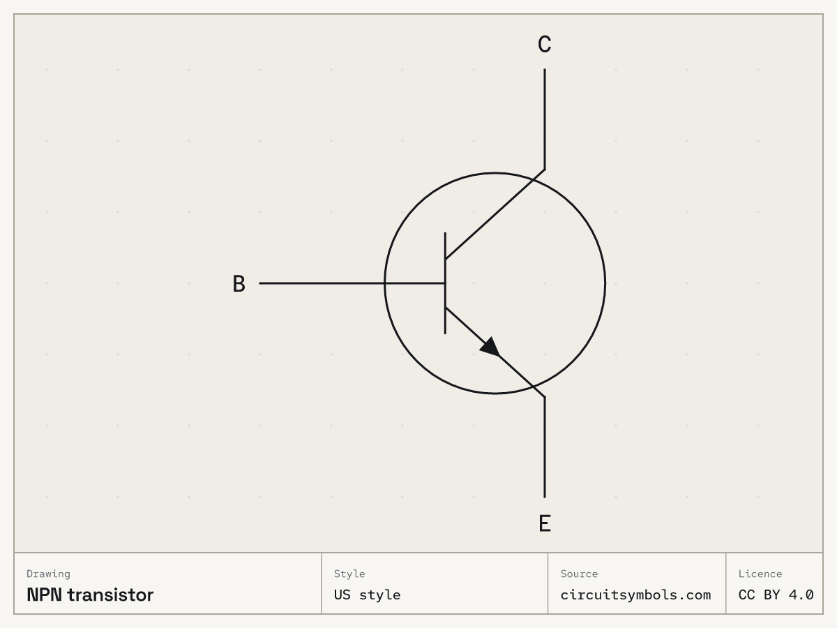 US style PNG, 1200 × 900 SVG, line art
 -
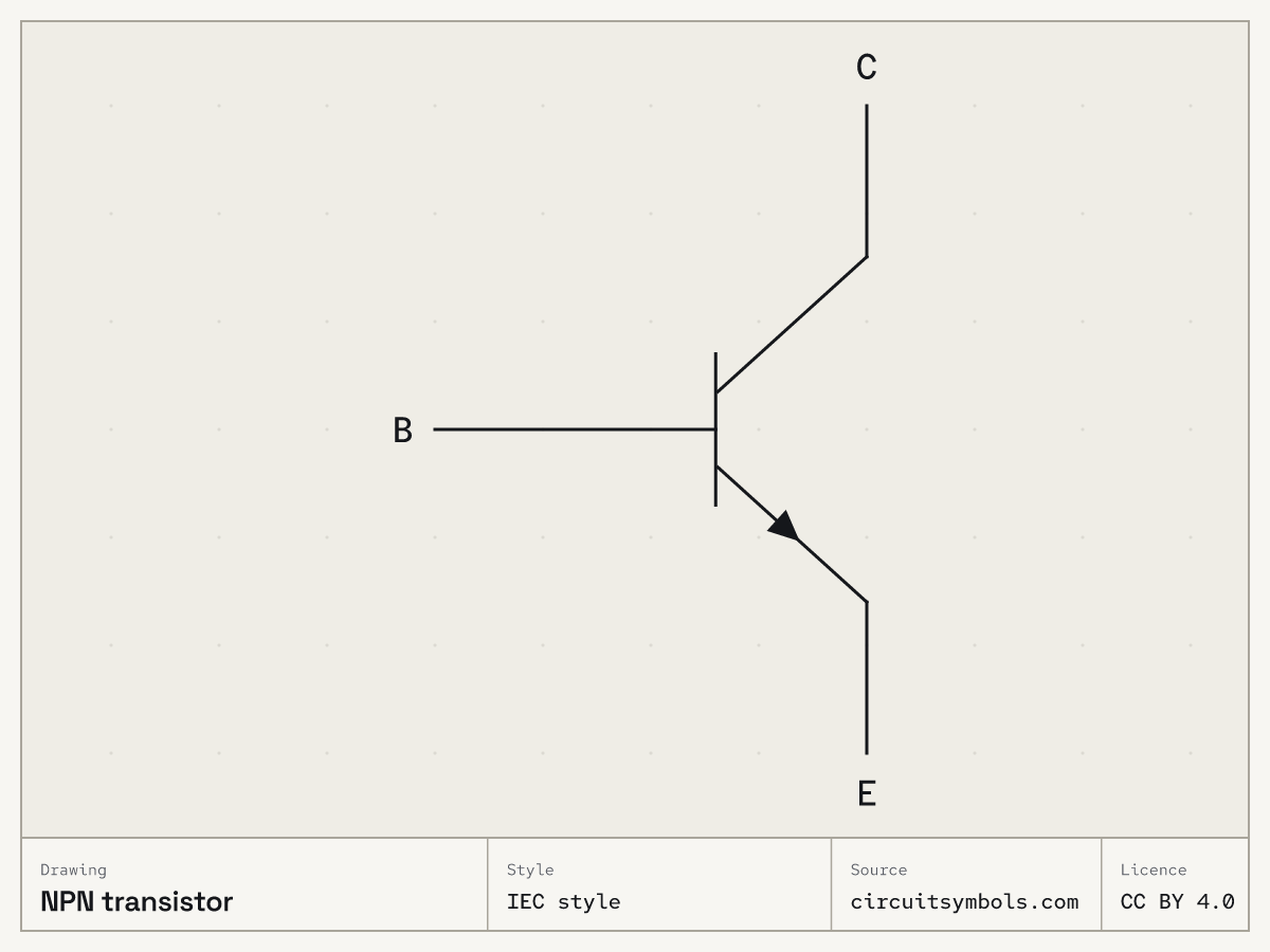 IEC style PNG, 1200 × 900 SVG, line art
Variants as SVG line art: PNP transistorPNP transistor, N-channel MOSFETN-channel MOSFET, P-channel MOSFETP-channel MOSFET
Sources
15 sources, numbered as cited
- ModEL — Bipolar Junction Transistors, simplified tutorial and §4.2 (terminal roles)
- Lessons In Electric Circuits, Vol. V — §9, Circuit Schematic Symbols (pp. 130–139)
- ModEL — Field-Effect Transistors, §4.3 and §6.2 (body, channel and symbol alternatives)
- ModEL — Bipolar Junction Transistors, §4.3 note 8 (emitter arrow direction, p. 32)
- Design to Manufacturing Standards — Reference Designators (slide 33)
- E84 — Bipolar Junction Transistor: terminals and optional symbol enclosure
- ModEL — Bipolar Junction Transistors, simplified tutorial (current directions and the emitter arrow, p. 20)
- Lessons In Electric Circuits, Vol. III — §2.8, bipolar junction transistors (emitter arrow, p. 63)
- Electrical Schematics, §§1.3.1–1.3.5 — nodes, crossings, references and congruent drawings
- ModEL — PN Junctions and Diodes, §§2.3–2.7 (bias and diode variants)
- ModEL — Components and Symbols, §3.16 (diodes, p. 29)
- Diodes — terminal polarity, ideal and offset models (pp. 1–2, 7–10)
- ModEL — Semiconductor Logic Gates, §2.1 (schematic versus package pinout, p. 8)
- ModEL — Electromechanical Relays, §§3.2–3.3 and §5.1 (normal and present contact status)
- ModEL — Transistor Switching Circuits, §§3.1–3.4 (cutoff and saturation)