Circuit symbols chart
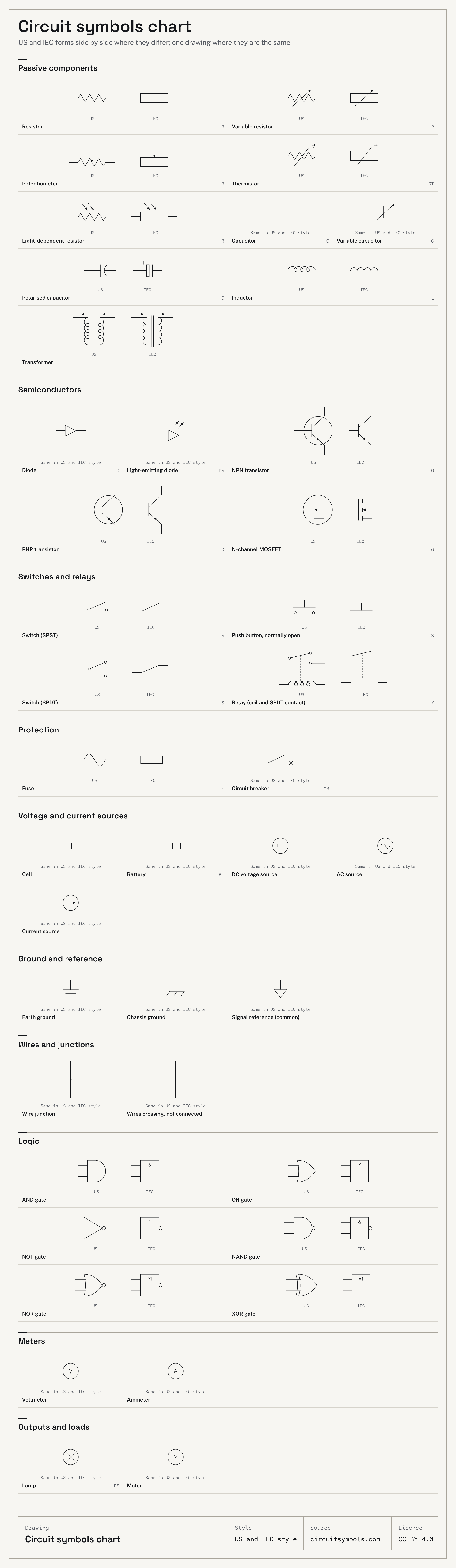
52 symbols in US and IEC style: 41 on the chart at one drawing scale, and 11 more variants from the symbol sheets.
Circuit symbols are the drawings a schematic uses for parts and their connections. Some differ between US and IEC style, such as the resistor’s zigzag and rectangle, and the coil’s loops and humps. Each row on this chart names a drawing and its meaning.Source 1Source 2Source 3Source 4Source 5Source 6
Resistor R
US | IEC Both styles, yours first.
Name, letter Select a cell for more. A letter shows only where a cited source names one.
No symbol on this chart matches that search, and some symbols are not drawn on this site yet. Try the A–Z index of names and other names, the glossary, or the symbol sheets listed at the foot of the page.
Passive components
15 symbols
-
Resistor
Designator R
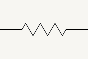
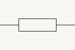
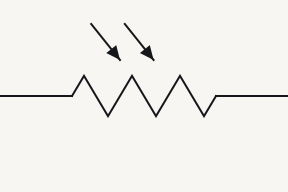
A resistor symbol stands for a component that opposes current. The zigzag (US style) and the plain rectangle (IEC style) are two drawings of the same component.
Terminals 1, 2
- 1, 2
- A fixed resistor has two interchangeable terminals; the symbol has no polarity.
-
Variable resistor
Designator R
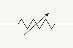
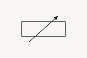
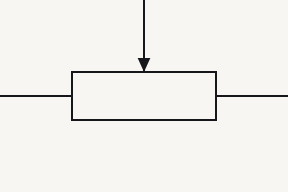
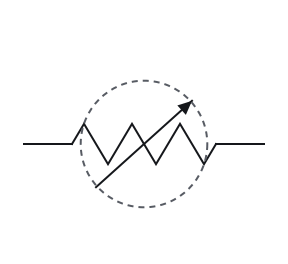
A diagonal arrow through the resistor body marks a variable resistor.
Terminals 1, 2
- 1, 2
- This symbol has two terminals and no polarity mark. The labels 1 and 2 only tell the two ends apart.
-
Potentiometer
Designator R
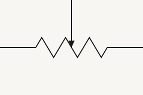
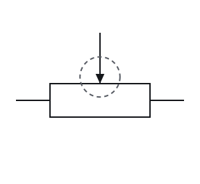
A potentiometer has three terminals: the two ends of the resistive track and a wiper, drawn as an arrow touching the body.
Terminals 1, W, 2
- 1, 2
- Terminals 1 and 2 are the fixed terminals, one at each end of the resistive track.
- W
- W is the wiper: the movable third terminal, drawn as the arrow touching the body. It makes contact wherever it rests along the track.
-
Thermistor
Designator RT
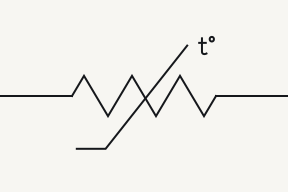
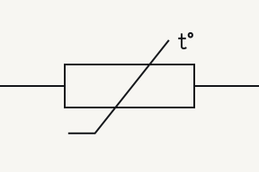
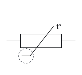
A thermistor's resistance changes with temperature. NTC resistance falls as temperature rises; PTC resistance rises. A generic thermistor symbol without a type label does not distinguish the two.
Terminals 1, 2
- 1, 2
- This symbol has two terminals and no polarity mark. The labels 1 and 2 only tell the two ends apart.
-
LDR (light-dependent resistor)
Designator R
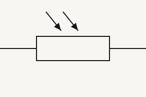
Two arrows arriving at a resistor body mark a light-dependent resistor (photoresistor).
Terminals 1, 2
- 1, 2
- This symbol has two terminals and no polarity mark. The labels 1 and 2 only tell the two ends apart.
-
Capacitor
Designator C
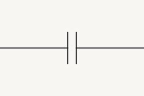
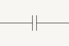
A capacitor symbol stands for two conductors separated by an insulator; the two parallel plates are a picture of that.
Terminals 1, 2
- 1, 2
- A non-polarised capacitor has two interchangeable terminals.
-
Polarised (polarized) capacitor
Designator C
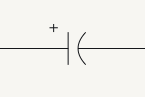
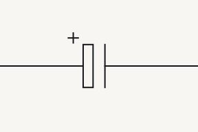
In the polarised capacitor drawings here, + marks the positive terminal. The US form has a curved negative plate; the IEC form has a hollow positive plate. The marked polarity must be respected.
Terminals +, −
- +
- The + terminal is the one the polarity mark names as positive. In the US form here it connects to the straight plate; in the IEC form, to the hollow plate.
- −
- The − terminal is the other side of the marked polarity. In the US form here it connects to the curved plate; in the IEC form, to the plate opposite the hollow one.
-
Variable capacitor
Designator C
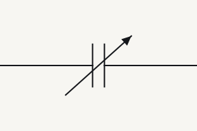
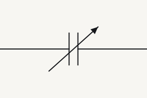
In the variable-capacitor convention used here, a diagonal arrow through the plates indicates adjustable capacitance.
Terminals 1, 2
- 1, 2
- A non-polarised capacitor has two interchangeable terminals.
-
Inductor
Designator L
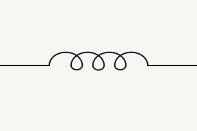
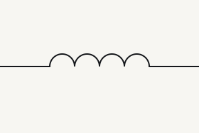
An inductor stores energy in a magnetic field and opposes changes in current; its symbol represents the coil.
Terminals 1, 2
- 1, 2
- The plain, uncoupled two-terminal inductor symbol has no fixed polarity mark; either terminal can be used as the voltage reference.
-
Transformer
Designator T
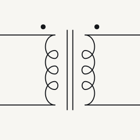
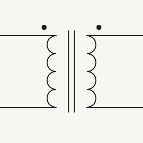
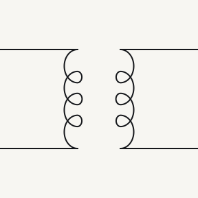
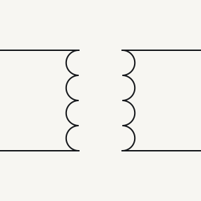
The separate-winding transformer shown here transfers energy magnetically between windings without an internal conducting connection between them. This description excludes an autotransformer, whose windings share a conducting connection.
Terminals P1, P2, S1, S2
- P1, P2
- The primary winding is the one driven by the source.
- S1, S2
- The secondary winding is the one that delivers power to the load.
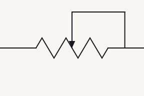
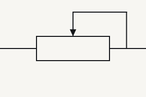
Also drawn on the resistor sheet
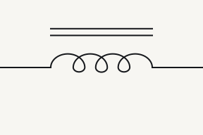
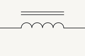
Also drawn on the inductor sheet
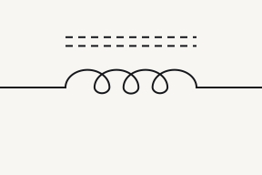
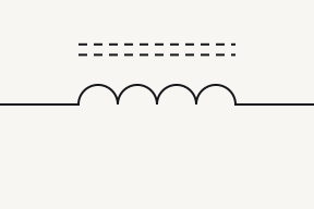
Also drawn on the transformer sheet
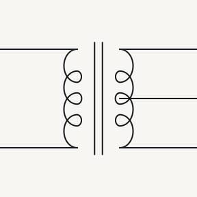
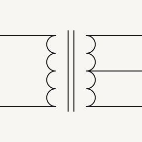
Semiconductors
9 symbols
-
Diode
Designator D
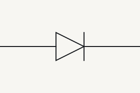
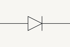
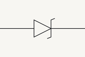
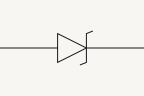
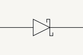
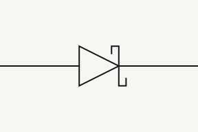
A diode conducts much more readily in its forward direction than in its reverse direction. Real devices also have leakage and reverse breakdown, which this page's simplified models omit.
Terminals A, K
- A
- The anode (A) is the terminal opposite the bar. During forward conduction, conventional current enters the diode at the anode.
- K
- The cathode (K) is the terminal at the bar. During forward conduction, conventional current leaves the diode at the cathode.
-
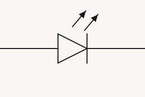
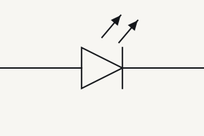
LED (light-emitting diode)
Designator DS
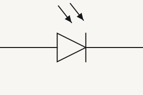
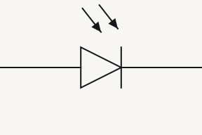
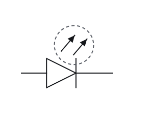
Two arrows leaving the diode body mark a light-emitting diode.
Terminals A, K
- A
- The anode (A) is the terminal opposite the bar. During forward conduction, conventional current enters the diode at the anode.
- K
- The cathode (K) is the terminal at the bar. During forward conduction, conventional current leaves the diode at the cathode.
-
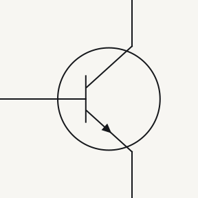
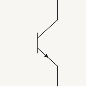
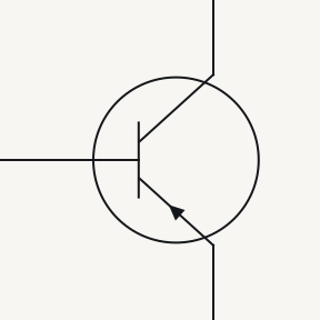
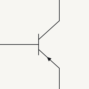
NPN transistor
Designator Q
A bipolar transistor has base, collector and emitter terminals. In the current-controlled model used here, base drive controls conduction between collector and emitter.
Terminals B, C, E
- B
- The base is the terminal drawn against the flat bar; a small base current controls the device.
- C
- The collector is the branch connected to the base bar that has no emitter arrow. The base has its own separate lead to that bar.
- E
- The arrow is always on the emitter. It points out of the transistor for NPN and into it for PNP, whichever way the symbol is rotated.
-
PNP transistor
Designator Q
The arrow is always on the emitter. It points out of the transistor for NPN and into it for PNP, whichever way the symbol is rotated.
Terminals B, C, E
- B
- The base is the terminal drawn against the flat bar; a small base current controls the device.
- C
- The collector is the branch connected to the base bar that has no emitter arrow. The base has its own separate lead to that bar.
- E
- The arrow is always on the emitter. It points out of the transistor for NPN and into it for PNP, whichever way the symbol is rotated.
-
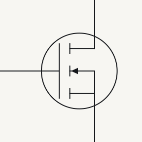
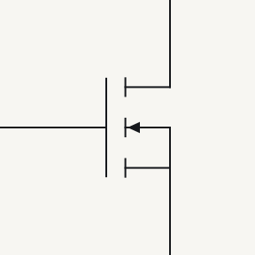
N-channel MOSFET
Designator Q
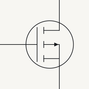
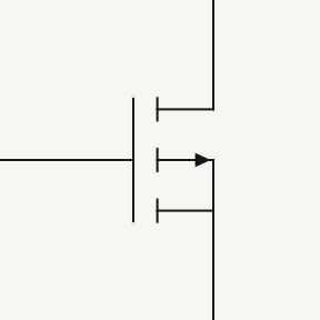
A MOSFET uses gate voltage relative to source to control its channel between drain and source. The three-terminal form shown here connects its body internally to source.
Terminals G, D, S
- G
- The gate is the insulated terminal drawn parallel to the channel with a gap between them.
- D
- The drain (D) is the other channel terminal: the channel runs between drain and source.
- S
- The source (S) is the channel terminal joined to the body in the three-terminal form shown here, so the controlling gate voltage is applied between gate and source.
Also drawn on the diode sheet
Also drawn on the transistor sheet
Switches and relays
6 symbols
-
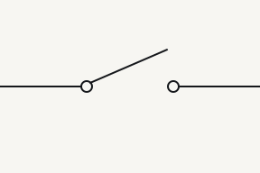
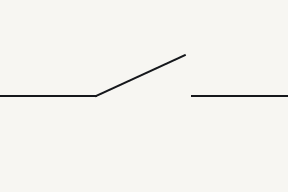
Switch (SPST)
Designator S
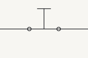
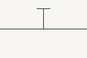
A switch symbol stands for a contact that either completes or breaks a path.
Terminals 1, 2
- 1, 2
- A single-pole, single-throw (SPST) switch has two terminals. Their left or right position on the page does not give them different electrical roles.
-
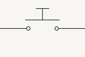
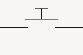
Push button, normally open
Designator S
The momentary push buttons shown here change contact state while pressed and return to their drawn, unactuated state when released.
Terminals 1, 2
- 1, 2
- A single-pole, single-throw (SPST) switch has two terminals. Their left or right position on the page does not give them different electrical roles.
-
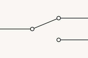
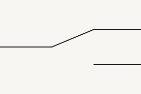
Switch (SPDT)
Designator S
Poles count the separate circuits a switch controls; throws count the contact destinations available to each pole. An off position is not an additional throw.
Terminals COM, 1, 2
- COM
- In a double-throw switch the common terminal is the one the moving arm belongs to.
- 1, 2
- Each throw terminal is one of the positions the arm can connect the common terminal to.
-
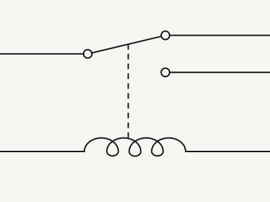
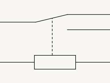
Relay (coil and SPDT contact)
Designator K
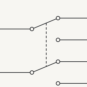
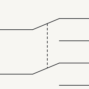
The electromechanical relay shown here uses a coil to move contacts. Its coil circuit is electrically separate from the switched contact circuit.
Terminals COM, NC, NO, A1, A2
- COM
- COM is the common contact, the one the moving arm belongs to.
- NC
- NC is the normally-closed contact: it is connected to COM in the resting, de-energised state of the single-stable relay shown here.
- NO
- NO is the normally-open contact: it is disconnected from COM at rest and connected after the coil has energised the single-stable relay shown here.
- A1, A2
- The two coil terminals are the control side of the relay; the current that flows through them moves the contacts.
Also drawn on the switch sheet
Protection
2 symbols
-
Fuse
Designator F
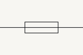
A fuse opens a conducting link when sufficient overcurrent heats the link until it melts.
Try the inputsTerminals 1, 2
- 1, 2
- The simple fuse-link symbol shown here has two terminals and no polarity mark.
-
Circuit breaker
Designator CB
The overcurrent circuit breaker represented here opens its contacts automatically on overcurrent and can be reset.
Terminals 1, 2
- 1, 2
- This symbol has two terminals and no polarity mark. The labels 1 and 2 only tell the two ends apart.
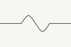
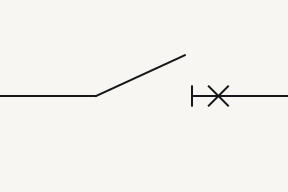
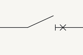
Voltage and current sources
5 symbols
-
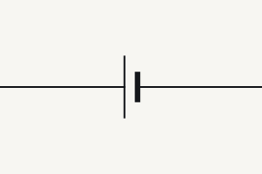
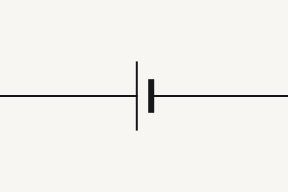
Cell
In a cell symbol the long thin line is the positive terminal and the short thick line is the negative terminal.
Terminals +, −
- +
- The + mark identifies the higher-potential terminal relative to the − terminal. The polarity marks alone do not determine whether current is entering or leaving the source.
- −
- The − mark identifies the lower-potential terminal relative to the + terminal. It is not automatically the circuit's zero-volt reference.
-
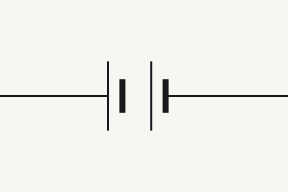
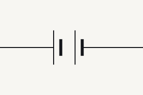
Battery
Designator BT
A battery is drawn as several cells in a row; the terminals follow the same long-positive rule.
Terminals +, −
- +
- The + mark identifies the higher-potential terminal relative to the − terminal. The polarity marks alone do not determine whether current is entering or leaving the source.
- −
- The − mark identifies the lower-potential terminal relative to the + terminal. It is not automatically the circuit's zero-volt reference.
-
DC voltage source
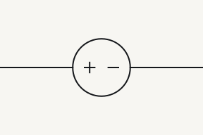
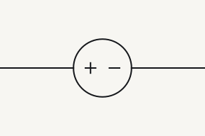
The generic DC voltage-source drawing used in both views is a circle with + and − signs. An ideal voltage source fixes the voltage difference between those terminals.
Terminals +, −
- +
- The + mark identifies the higher-potential terminal relative to the − terminal. The polarity marks alone do not determine whether current is entering or leaving the source.
- −
- The − mark identifies the lower-potential terminal relative to the + terminal. It is not automatically the circuit's zero-volt reference.
-
AC source
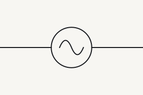
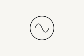
The sinusoidal AC voltage-source drawing used here is a circle with a sine wave inside.
Terminals 1, 2
- 1, 2
- The sinusoidal AC voltage source shown here alternates its polarity between its two terminals; neither terminal is permanently positive.
-
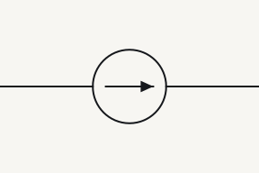
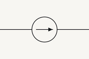
Current source
The generic current-source drawing used in both views is a circle with an arrow giving conventional current direction. An ideal current source fixes that current; the arrow does not give voltage polarity.
Terminals 1, 2
- 1
- Conventional current enters the ideal current source at the tail end of its arrow; this does not specify that terminal's voltage polarity.
- 2
- Conventional current leaves the ideal current source at the arrowhead end; this does not specify that terminal's voltage polarity.
Ground and reference
3 symbols
-
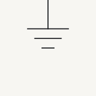
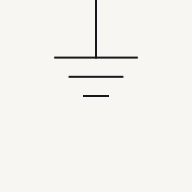
Earth ground
In the convention used here, three horizontal lines of decreasing length identify a connection to earth. Check a drawing's legend: the same shape is sometimes used more generally for circuit ground.
Terminals 1
- 1
- Each ground or reference symbol shown here has one connection point to the circuit; it identifies a reference connection, not a two-terminal component.
-
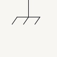
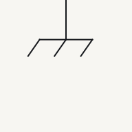
Chassis ground
The chassis symbol (hatched) marks a connection to the equipment's metal frame or enclosure.
Terminals 1
- 1
- Each ground or reference symbol shown here has one connection point to the circuit; it identifies a reference connection, not a two-terminal component.
-
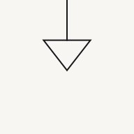
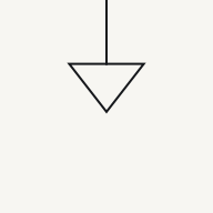
Signal reference (common)
The signal-reference symbol marks the chosen zero-volt reference for circuit voltages. It need not be connected to earth or chassis.
Terminals 1
- 1
- Each ground or reference symbol shown here has one connection point to the circuit; it identifies a reference connection, not a two-terminal component.
Wires and junctions
2 symbols
-
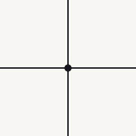
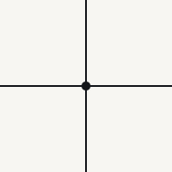
Wire junction
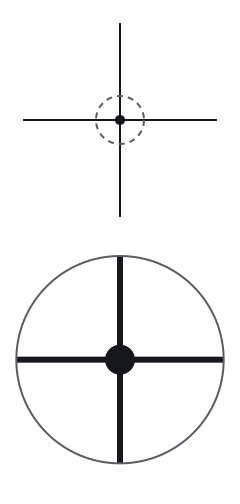
In the drawing convention used here, a dot marks a wire connection and a plain four-way crossing without a dot is not connected. Older drawings may use another convention, so check their legend.
-
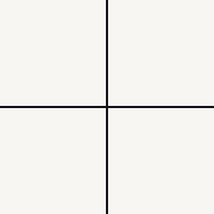
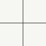
Wires crossing, not connected
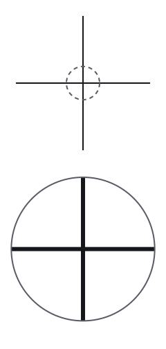
In the newer convention used here, wires that cross with no dot are not connected. Older schematics drew connected wires as a plain crossing and made unconnected wires hop over each other with a small half-circle, so check a drawing's legend.
Logic
6 symbols
-
AND gate
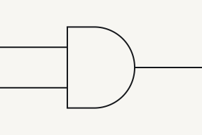
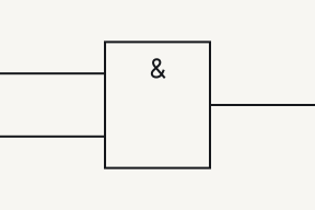
An AND gate's output is 1 only when every input is 1.
Try the inputsTerminals A, B, Y
- A, B
- In the unrotated gate drawings here, inputs appear on the left. Each input is a logic value, 0 or 1; rotating the symbol does not turn an input into an output.
- Y
- In the unrotated gate drawings here, the output appears on the right. Its settled logic value follows the gate's truth table.
-
OR gate
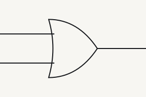
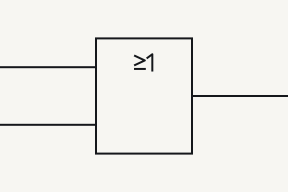
An OR gate's output is 1 when any input is 1.
Try the inputsTerminals A, B, Y
- A, B
- In the unrotated gate drawings here, inputs appear on the left. Each input is a logic value, 0 or 1; rotating the symbol does not turn an input into an output.
- Y
- In the unrotated gate drawings here, the output appears on the right. Its settled logic value follows the gate's truth table.
-
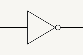
NOT gate
A NOT gate's output is the opposite of its input.
Try the inputsTerminals A, Y
- A
- In the unrotated gate drawings here, inputs appear on the left. Each input is a logic value, 0 or 1; rotating the symbol does not turn an input into an output.
- Y
- In the unrotated gate drawings here, the output appears on the right. Its settled logic value follows the gate's truth table.
-
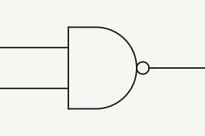
NAND gate
A NAND gate's output is 0 only when every input is 1.
Try the inputsTerminals A, B, Y
- A, B
- In the unrotated gate drawings here, inputs appear on the left. Each input is a logic value, 0 or 1; rotating the symbol does not turn an input into an output.
- Y
- In the unrotated gate drawings here, the output appears on the right. Its settled logic value follows the gate's truth table.
-
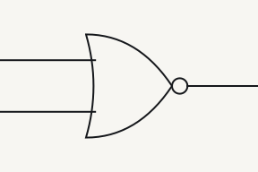
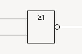
NOR gate
A NOR gate's output is 1 only when every input is 0.
Try the inputsTerminals A, B, Y
- A, B
- In the unrotated gate drawings here, inputs appear on the left. Each input is a logic value, 0 or 1; rotating the symbol does not turn an input into an output.
- Y
- In the unrotated gate drawings here, the output appears on the right. Its settled logic value follows the gate's truth table.
-
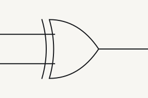
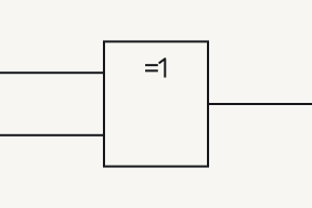
XOR gate
An exclusive-OR gate's output is 1 when its two inputs differ.
Try the inputsTerminals A, B, Y
- A, B
- In the unrotated gate drawings here, inputs appear on the left. Each input is a logic value, 0 or 1; rotating the symbol does not turn an input into an output.
- Y
- In the unrotated gate drawings here, the output appears on the right. Its settled logic value follows the gate's truth table.
Meters
2 symbols
-
Voltmeter
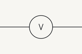
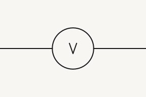
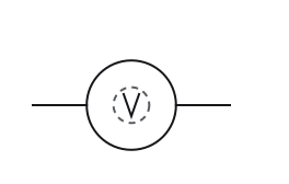
A voltmeter is drawn as a circle with a V and is connected across (in parallel with) the part it measures.
Terminals +, −
- +
- The + terminal marks the side a DC meter expects to be positive: its reading is positive when this terminal is at the higher potential.
- −
- The − terminal is the meter's other side. A DC meter reads positive when the + terminal is at a higher potential than this one.
-
Ammeter
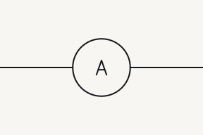
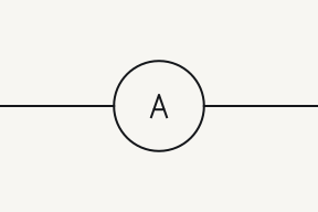
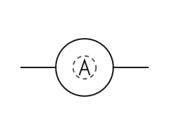
An ammeter is drawn as a circle with an A and is connected in line with (in series with) the current it measures.
Terminals +, −
- +
- The + terminal marks the side a DC meter expects to be positive: its reading is positive when this terminal is at the higher potential.
- −
- The − terminal is the meter's other side. A DC meter reads positive when the + terminal is at a higher potential than this one.
Outputs and loads
2 symbols
-
Lamp
Designator DS
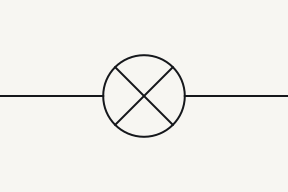
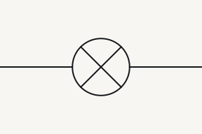
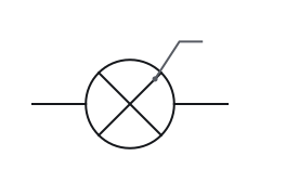
The incandescent-lamp convention used on this sheet is a circle with a cross inside.
Terminals 1, 2
- 1, 2
- This symbol has two terminals and no polarity mark. The labels 1 and 2 only tell the two ends apart.
-
Motor
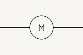
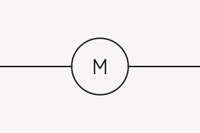
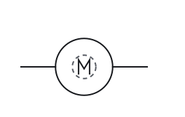
One common motor convention is a circle containing M; this sheet uses that form.
Terminals 1, 2
- 1, 2
- This symbol has two terminals and no polarity mark. The labels 1 and 2 only tell the two ends apart.
What changes between US and IEC
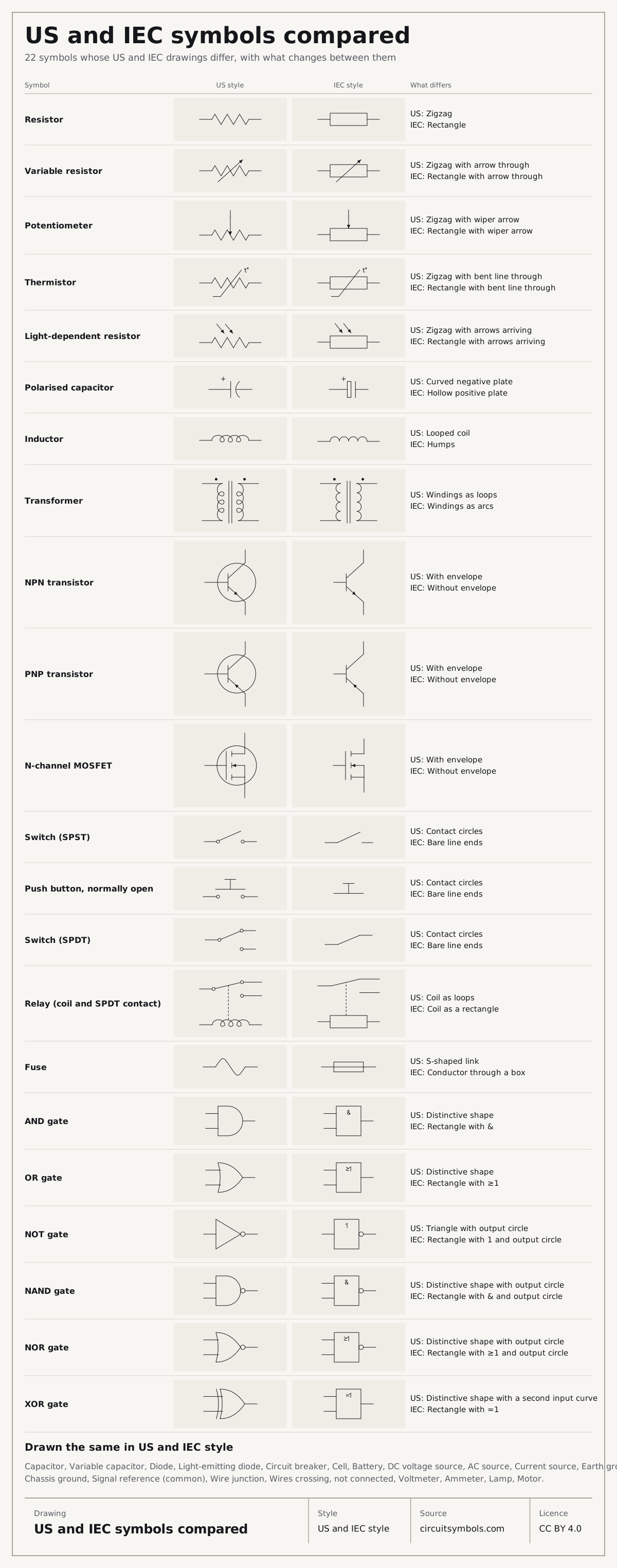
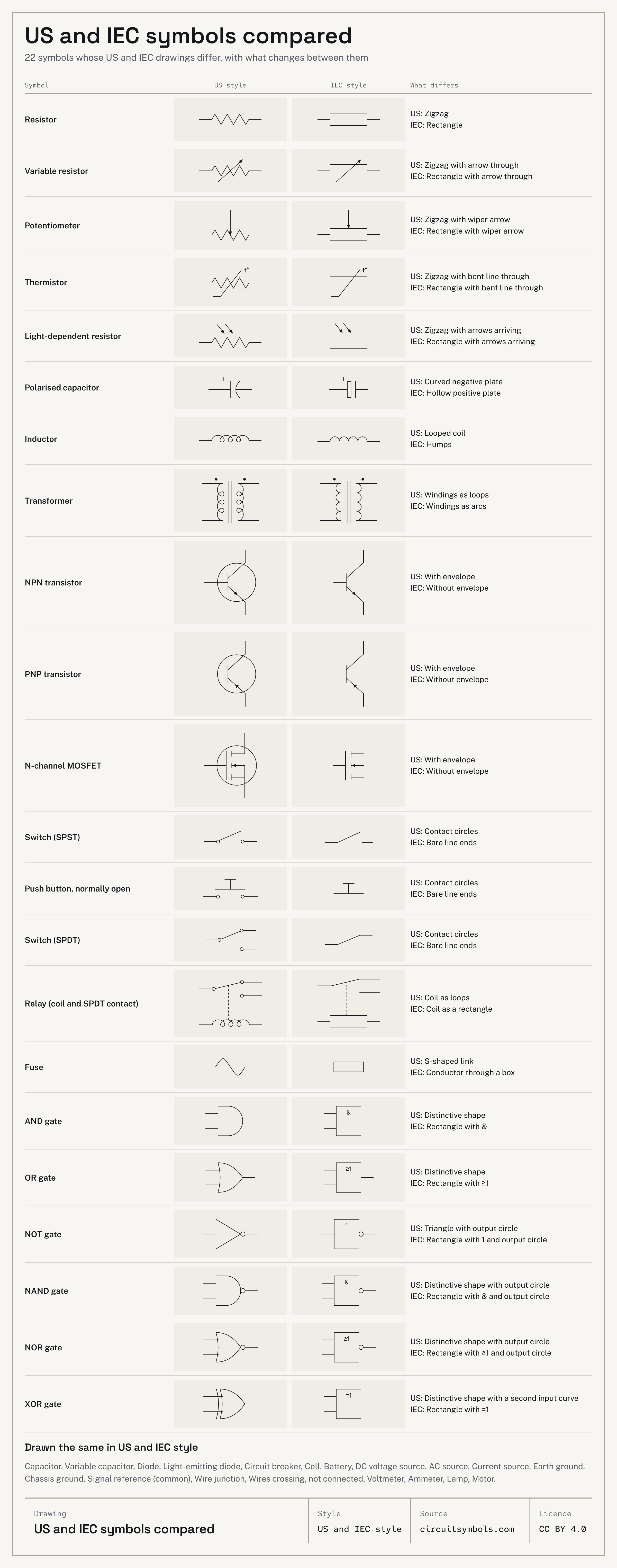
22 of the 41 symbols on the chart are drawn differently in the two styles, so the chart shows both. The table names what changes. The other 19 are drawn the same.
| Symbol | US style | IEC style |
|---|---|---|
| Resistor | Zigzag | Rectangle |
| Variable resistor | Zigzag with arrow through | Rectangle with arrow through |
| Potentiometer | Zigzag with wiper arrow | Rectangle with wiper arrow |
| Thermistor | Zigzag with bent line through | Rectangle with bent line through |
| LDR (light-dependent resistor) | Zigzag with arrows arriving | Rectangle with arrows arriving |
| Polarised (polarized) capacitor | Curved negative plate | Hollow positive plate |
| Inductor | Looped coil | Humps |
| Transformer | Windings as loops | Windings as arcs |
| NPN transistor | With envelope | Without envelope |
| PNP transistor | With envelope | Without envelope |
| N-channel MOSFET | With envelope | Without envelope |
| Symbol | US style | IEC style |
|---|---|---|
| Switch (SPST) | Contact circles | Bare line ends |
| Push button, normally open | Contact circles | Bare line ends |
| Switch (SPDT) | Contact circles | Bare line ends |
| Relay (coil and SPDT contact) | Coil as loops | Coil as a rectangle |
| Fuse | S-shaped link | Conductor through a box |
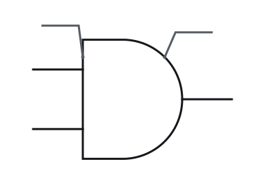
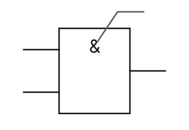
| AND gate | Distinctive shape | Rectangle with & |
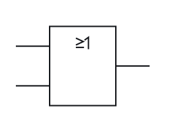
| OR gate | Distinctive shape | Rectangle with ≥1 |
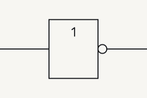
| NOT gate | Triangle with output circle | Rectangle with 1 and output circle |
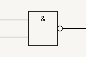
| NAND gate | Distinctive shape with output circle | Rectangle with & and output circle |
| NOR gate | Distinctive shape with output circle | Rectangle with ≥1 and output circle |
| XOR gate | Distinctive shape with a second input curve | Rectangle with =1 |
Symbols that look alike
Each figure rings the one mark that tells the drawings apart.
-
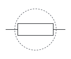
Resistor
Plain rectangle
-
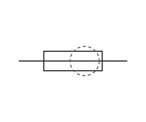
Fuse
A line running through it
-
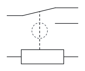
Relay (coil and SPDT contact)
Dashed line to a contact
Three IEC symbols are rectangles: a plain rectangle is a resistor, a rectangle with a line running through it end to end is a fuse, and a rectangle joined by a dashed line to a contact is a relay coil.Source 2Source 8Source 24
-
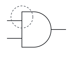
AND gate
Straight input side, rounded front
-
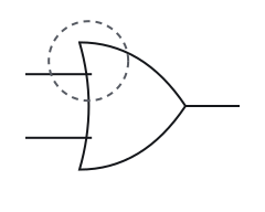
OR gate
Curved input side, pointed front
AND and OR differ in outline: the US AND shape has a straight input side and a rounded front, and the OR shape has a curved input side and a pointed front. In IEC boxes, & marks AND and ≥1 marks OR.Source 31Source 34
-
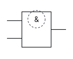
AND gate
&
-
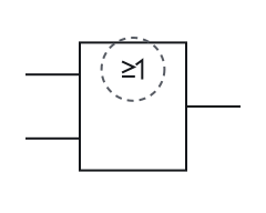
OR gate
≥1
AND and OR differ in outline: the US AND shape has a straight input side and a rounded front, and the OR shape has a curved input side and a pointed front. In IEC boxes, & marks AND and ≥1 marks OR.Source 31Source 34
-
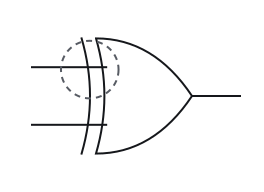
XOR gate
Second curved line
-
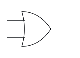
OR gate
XOR differs from OR by one mark: in the US shape a second curved line runs across the inputs, and in the IEC box =1 replaces ≥1.Source 31Source 35
-
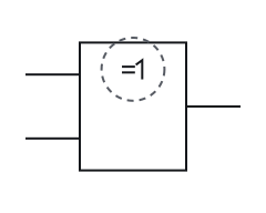
XOR gate
=1
-
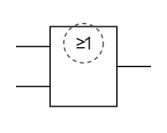
OR gate
≥1
XOR differs from OR by one mark: in the US shape a second curved line runs across the inputs, and in the IEC box =1 replaces ≥1.Source 31Source 35
-
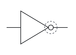
NOT gate
Circle on the output
-
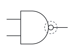
NAND gate
Circle on the output
-
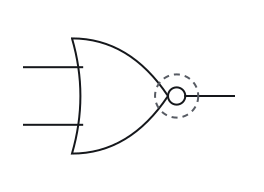
NOR gate
Circle on the output
-
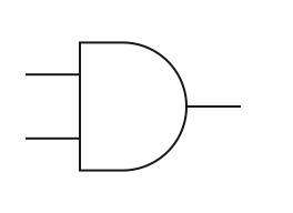
AND gate
-
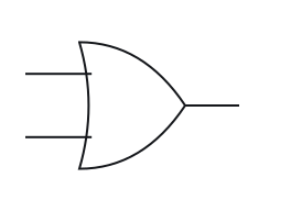
OR gate
NAND and NOR are the AND and OR shapes with a small circle on the output, and NOT is a triangle with that circle. In IEC boxes the same circle sits on the output. The circle marks inversion.Source 31Source 36Source 37
-
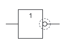
NOT gate
Circle on the output
-
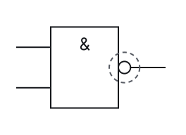
NAND gate
Circle on the output
-
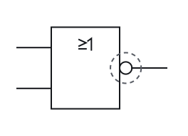
NOR gate
Circle on the output
-
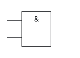
AND gate
-
OR gate
NAND and NOR are the AND and OR shapes with a small circle on the output, and NOT is a triangle with that circle. In IEC boxes the same circle sits on the output. The circle marks inversion.Source 31Source 36Source 37
-
Wire junction
The dot
-
Wires crossing, not connected
Wires that meet in a T are connected whether or not a dot is drawn there. Where four wires cross and connect, the dot is what shows it.Source 29
-
Voltmeter
V
-
Ammeter
A
-
Lamp
-
Motor
M
Several symbols are circles told apart by what is inside: V for a voltmeter, A for an ammeter, a cross for a lamp and M for a motor.Source 20Source 32Source 33
Marks a symbol adds
-
Variable resistor
Arrow through: adjustable
-
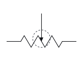
Potentiometer
Arrow that stops on the body: a wiper
-
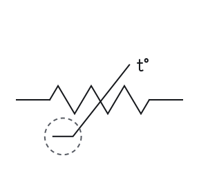
Thermistor
Short flat foot: resistance that changes with temperature
-
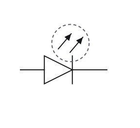
Light-emitting diode
Arrows leaving: light-emitting
-
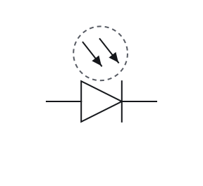
Photodiode
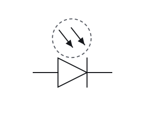
Arrows arriving: a photodiode
-
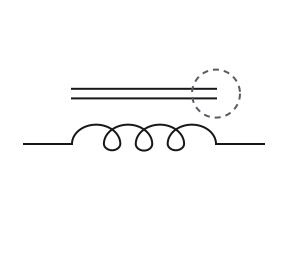
Iron-core inductor
Solid parallel core lines: iron
-
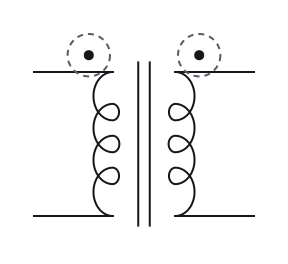
Transformer
Dots: corresponding voltage polarity
-
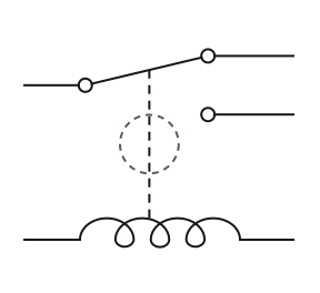
Relay (coil and SPDT contact)
Dashed line: a mechanical link
-
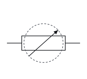
Variable resistor
Arrow through: adjustable
-
Potentiometer
Arrow that stops on the body: a wiper
-
Thermistor
Short flat foot: resistance that changes with temperature
-
Light-emitting diode
Arrows leaving: light-emitting
-
Photodiode
Arrows arriving: a photodiode
-
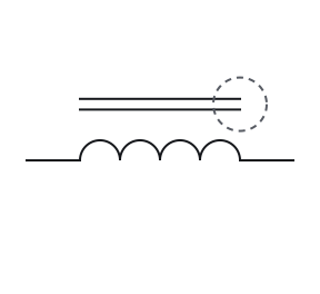
Iron-core inductor
Solid parallel core lines: iron
-
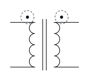
Transformer
Dots: corresponding voltage polarity
-
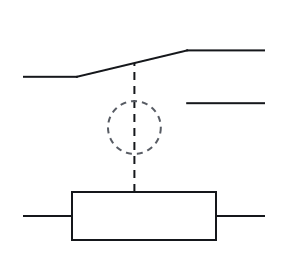
Relay (coil and SPDT contact)
Dashed line: a mechanical link
Fuse and logic gates, part by part
These symbols have no sheet of their own yet: their parts, then their inputs to try.
-
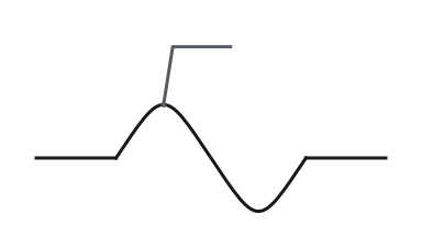
US style
-
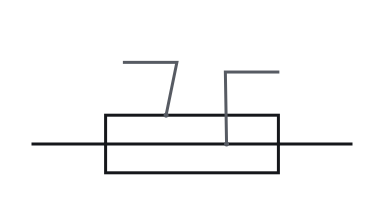
IEC style
- 1 Curved link
- 2 Rectangle
- 3 Conductor
- The two fuse forms used here are a curved link in the US view and a rectangle with a conductor through it in the IEC view. Both identify a fuse.Source 8
Fuse: try the states
Fuse
One node. Under the ideal fuse-link model, an intact fuse joins its two terminals with zero resistance, so they have the same potential.
No path. Under the ideal fuse-link model, a blown fuse has an open link and no conducting path through it. The printed symbol remains unchanged.
A fuse opens a conducting link when sufficient overcurrent heats the link until it melts.
Logic gates: try the inputs
AND gate
Y = 0. Under the two-input truth-table model, AND gives 0 when at least one input is 0.
Y = 0. Under the two-input truth-table model, AND gives 0 when at least one input is 0.
Y = 0. Under the two-input truth-table model, AND gives 0 when at least one input is 0.
Y = 1. Under the two-input truth-table model, AND gives 1 when both inputs are 1.
In the unrotated gate drawings here, the output appears on the right. Its settled logic value follows the gate's truth table.
| A | B | Output | Current row |
|---|---|---|---|
| 0 | 0 | Y = 0 | |
| 0 | 1 | Y = 0 | |
| 1 | 0 | Y = 0 | |
| 1 | 1 | Y = 1 |
NAND gate
Y = 1. Under the two-input truth-table model, NAND gives 1 when at least one input is 0.
Y = 1. Under the two-input truth-table model, NAND gives 1 when at least one input is 0.
Y = 1. Under the two-input truth-table model, NAND gives 1 when at least one input is 0.
Y = 0. Under the two-input truth-table model, NAND gives 0 when both inputs are 1.
In the gate conventions used here, a small output circle marks logical negation: it reverses the output's 0 or 1 value.
| A | B | Output | Current row |
|---|---|---|---|
| 0 | 0 | Y = 1 | |
| 0 | 1 | Y = 1 | |
| 1 | 0 | Y = 1 | |
| 1 | 1 | Y = 0 |
NOR gate
Y = 1. Under the two-input truth-table model, NOR gives 1 when both inputs are 0.
Y = 0. Under the two-input truth-table model, NOR gives 0 when at least one input is 1.
Y = 0. Under the two-input truth-table model, NOR gives 0 when at least one input is 1.
Y = 0. Under the two-input truth-table model, NOR gives 0 when at least one input is 1.
In the gate conventions used here, a small output circle marks logical negation: it reverses the output's 0 or 1 value.
| A | B | Output | Current row |
|---|---|---|---|
| 0 | 0 | Y = 1 | |
| 0 | 1 | Y = 0 | |
| 1 | 0 | Y = 0 | |
| 1 | 1 | Y = 0 |
NOT gate
Y = 1. Under the one-input truth-table model, NOT gives 1 when its input is 0.
Y = 0. Under the one-input truth-table model, NOT gives 0 when its input is 1.
In the gate conventions used here, a small output circle marks logical negation: it reverses the output's 0 or 1 value.
| A | Output | Current row |
|---|---|---|
| 0 | Y = 1 | |
| 1 | Y = 0 |
OR gate
Y = 0. Under the two-input truth-table model, OR gives 0 when both inputs are 0.
Y = 1. Under the two-input truth-table model, OR gives 1 when at least one input is 1.
Y = 1. Under the two-input truth-table model, OR gives 1 when at least one input is 1.
Y = 1. Under the two-input truth-table model, OR gives 1 when at least one input is 1.
In the unrotated gate drawings here, the output appears on the right. Its settled logic value follows the gate's truth table.
| A | B | Output | Current row |
|---|---|---|---|
| 0 | 0 | Y = 0 | |
| 0 | 1 | Y = 1 | |
| 1 | 0 | Y = 1 | |
| 1 | 1 | Y = 1 |
XOR gate
Y = 0. Under the two-input truth-table model, XOR gives 0 when the inputs are equal.
Y = 1. Under the two-input truth-table model, XOR gives 1 when the inputs differ.
Y = 1. Under the two-input truth-table model, XOR gives 1 when the inputs differ.
Y = 0. Under the two-input truth-table model, XOR gives 0 when the inputs are equal.
In the unrotated gate drawings here, the output appears on the right. Its settled logic value follows the gate's truth table.
| A | B | Output | Current row |
|---|---|---|---|
| 0 | 0 | Y = 0 | |
| 0 | 1 | Y = 1 | |
| 1 | 0 | Y = 1 | |
| 1 | 1 | Y = 0 |
Print the chart
Printing gives the view on screen, chart or details, in both drawing styles and without the find bar. To keep a PDF, choose Save as PDF in your print dialog. For one family, labelled or blank, use the worksheets.
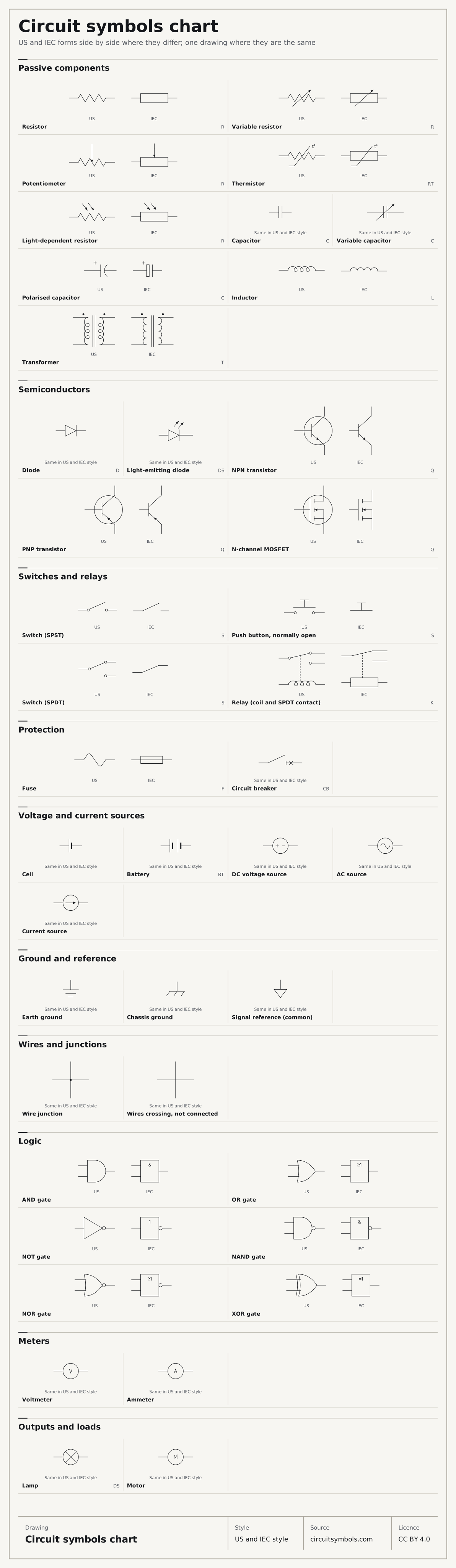
Open the full sheet (SVG) Download PNG, 2400 px
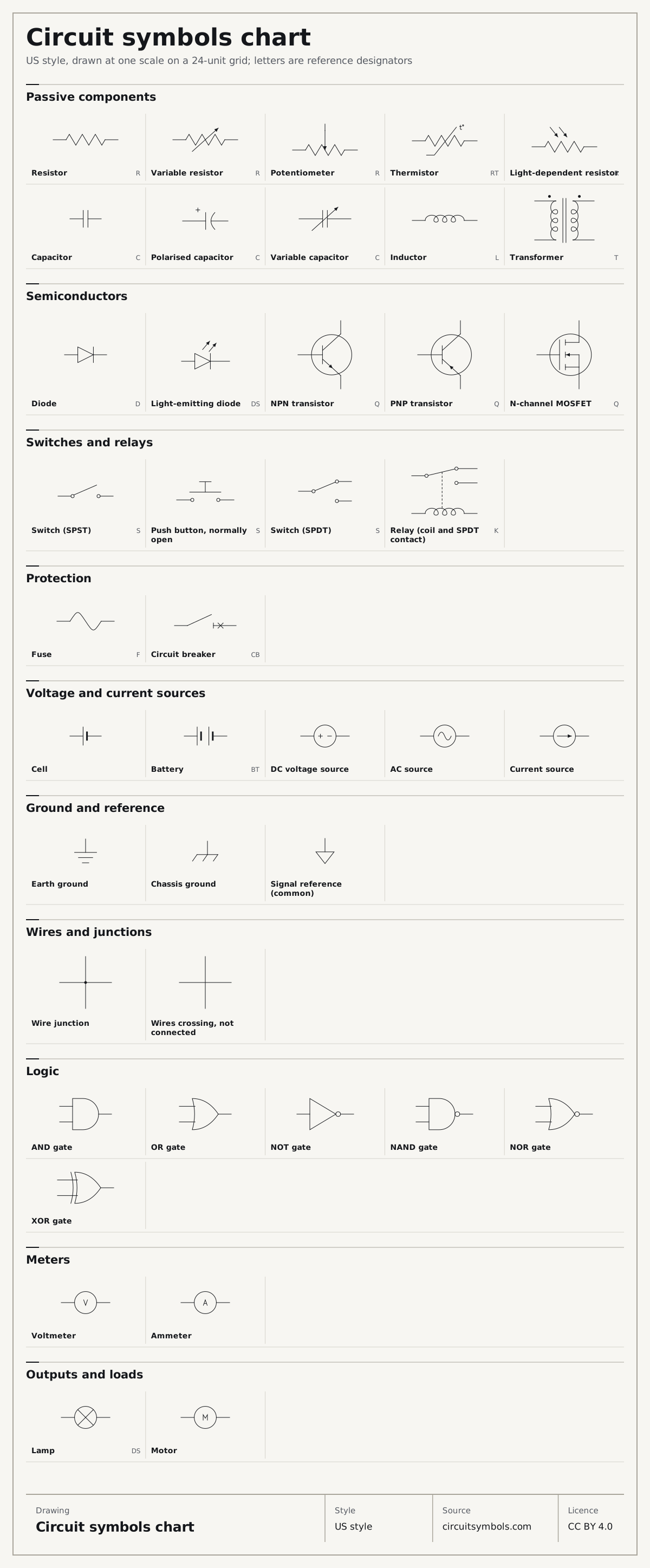
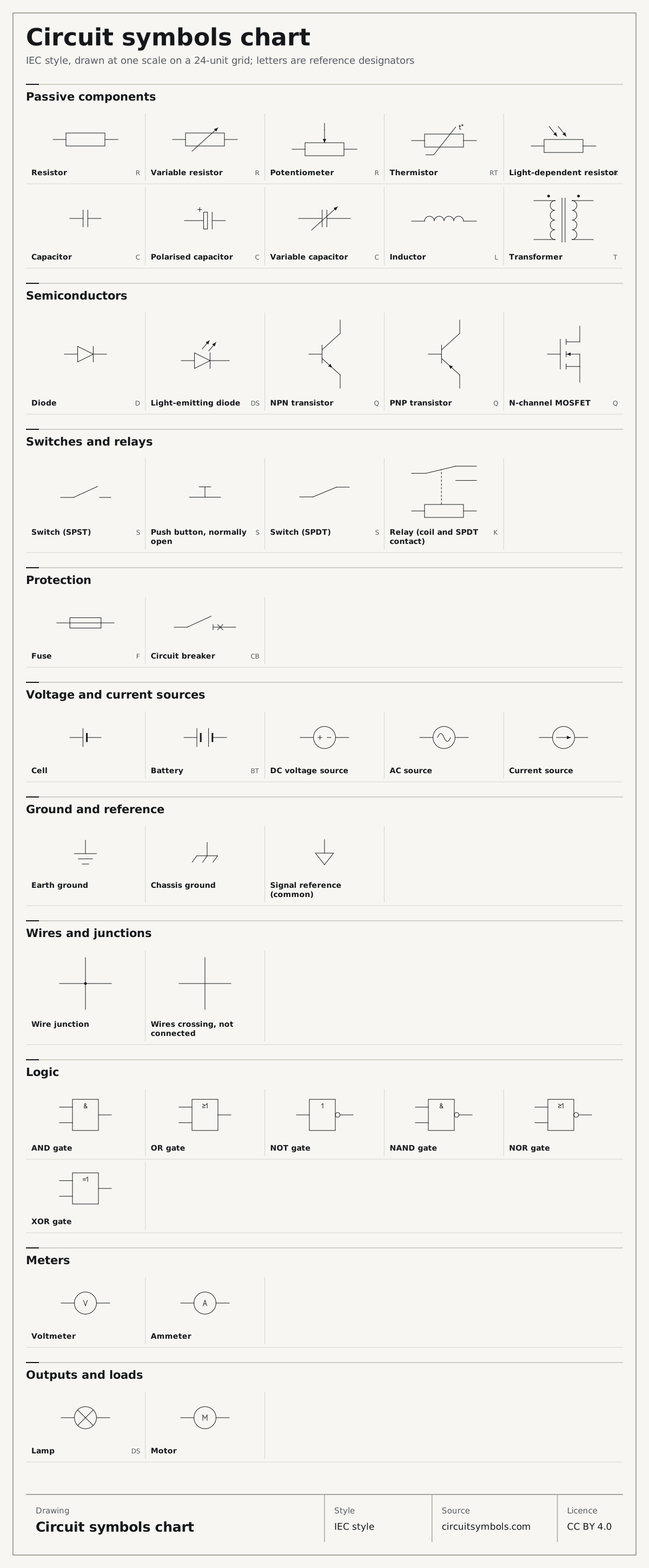
One style only: US chart (SVG) or IEC chart (SVG). The US and IEC comparison as one sheet: SVG or PNG, 2400 px.
A–Z index
52 symbols and 51 other names
0–9
- 0 V reference see Signal reference (common)
A
- AC source
- AC voltage source see AC source
- Air-core transformer
- Ammeter
- AND gate
C
- Capacitor
- Cell
- Center tap transformer see Centre-tapped transformer
- Centre-tapped transformer
- Changeover switch see Switch (SPDT)
- Chassis ground
- Circuit breaker
- Coil see Inductor
- Common see Signal reference (common)
- Connected wires see Wire junction
- Current source
D
- DC power supply see DC voltage source
- DC voltage source
- Diode
- Double pole double throw see Switch (DPDT)
- DPDT switch see Switch (DPDT)
E
- Earth see Earth ground
- Earth ground
- Electrolytic capacitor see Polarised (polarized) capacitor
- Electromechanical relay see Relay (coil and SPDT contact)
- Exclusive OR see XOR gate
F
- Ferrite-core inductor
- Fixed resistor see Resistor
- Frame ground see Chassis ground
- Fuse
G
- Ground see Earth ground; Chassis ground; Signal reference (common)
I
- Inductor
- Inverter see NOT gate
- Iron-core inductor
L
- Lamp
- LDR see LDR (light-dependent resistor)
- LDR (light-dependent resistor)
- LED see LED (light-emitting diode)
- LED (light-emitting diode)
- Light-dependent resistor see LDR (light-dependent resistor)
- Light-emitting diode see LED (light-emitting diode)
M
- Momentary switch see Push button, normally open
- MOSFET see N-channel MOSFET
- Motor
N
- N-channel MOSFET
- NAND gate
- NC push button see Push button, normally closed
- Non-polarised capacitor see Capacitor
- NOR gate
- Normally closed see Push button, normally closed
- Normally open contact see Push button, normally open
- NOT gate
- NPN transistor
- NTC see Thermistor
O
P
- P-channel MOSFET
- Photodiode
- Photoresistor see LDR (light-dependent resistor)
- PNP transistor
- Polarised (polarized) capacitor
- Polarised capacitor see Polarised (polarized) capacitor
- Polarized capacitor see Polarised (polarized) capacitor
- Pot see Potentiometer
- Potentiometer
- PTC see Thermistor
- Push button see Push button, normally open
- Push button, normally closed
- Push button, normally open
R
- Rectifier diode see Diode
- Relay see Relay (coil and SPDT contact)
- Relay (coil and SPDT contact)
- Resistor
- Rheostat
S
- Schottky diode
- Signal ground see Signal reference (common)
- Signal reference (common)
- Single cell see Cell
- Single pole double throw see Switch (SPDT)
- Single pole single throw see Switch (SPST)
- SPDT switch see Switch (SPDT)
- SPST switch see Switch (SPST)
- Switch see Switch (SPST); Push button, normally open; Push button, normally closed; Switch (SPDT); Switch (DPDT)
- Switch (DPDT)
- Switch (SPDT)
- Switch (SPST)
T
- Thermistor
- Transformer
- Transistor see NPN transistor; PNP transistor; N-channel MOSFET; P-channel MOSFET
- Trimmer capacitor see Variable capacitor
U
- Unconnected wires see Wires crossing, not connected
V
- Variable capacitor
- Variable resistor
- Voltage source see DC voltage source
- Voltmeter
W
- Wire crossing see Wires crossing, not connected
- Wire junction
- Wires crossing, not connected
X
How to use a legend
Five questions on reading a legend-
Match the shape
Look at the outline first, then at the small marks inside it: an arrow, a bar, a dot, a letter. The chart groups symbols by what they do, and the find bar also takes shape words such as zigzag, rectangle or loop.
-
Read the letter beside it
Reference designators identify parts with class letters and a number. Common letters used here are R resistor, C capacitor, D diode, Q transistor, L inductor, T transformer, S switch, K relay and F fuse; other naming systems exist.Source 7
-
Check how the drawing shows connections
The junction and crossing cells show the dot convention used here. A small half-circle hop where one wire passes over another also means the wires are not connected. Some drawings put a hop at every unconnected crossing and a dot at every connection, so neither is left to guess.Source 6Source 29Source 40
-
Tell parts from nodes
A ground or reference symbol marks a connection to the circuit's common reference, not a part, so the drawings here give it no reference designator. A label such as GND or 0 V names that node instead.Source 5Source 7Source 26
-
Keep the symbol and the part apart
A schematic symbol shows how terminals connect, not where they are on a real part. Terminal letters such as E, B and C or A and K do not give lead order or package layout; the part's own documentation does.Source 21Source 29Source 41
Questions
- Why do some symbols have two drawing forms?
- Two drawing conventions are in common use. A resistor may be a US-style zigzag or an IEC-style rectangle; it is the same component with the same terminals either way.Source 1Source 2Source 3Source 4Source 5
- Does turning a symbol round change the component?
- No. Rotating or mirroring the whole drawing, with its terminal labels and connections moving with it, leaves the component and its terminal roles as they were.Source 29
Sources
41 sources, numbered as cited
- IEEE 315-1975 — historical standard status
- ModEL — Components and Symbols, §§3.4–3.6 (NEMA and IEC symbol families, pp. 11–13)
- IEC 60617:2026 DB — Graphical symbols for diagrams
- ModEL — Components and Symbols, §§3.6–3.7 (resistors and potentiometers, pp. 13–14)
- DC Electrical Circuit Analysis — resistive devices and schematic ground symbols (pp. 53, 59–64)
- Lessons In Electric Circuits, Vol. V — §9, Circuit Schematic Symbols (pp. 130–139)
- Design to Manufacturing Standards — Reference Designators (slide 33)
- ModEL — Components and Symbols, §3.10 (fuses and circuit breakers, p. 20)
- ModEL — Components and Symbols, §3.11 (relay example with motor and lamp loads, p. 22)
- Thermistors — NTC and PTC product-description definitions
- ModEL — Components and Symbols, §3.15 (capacitor polarity, pp. 27–28)
- University Physics, Vol. 2, §8.1 — capacitor representations, Figure 8.9
- ModEL — Inductors and Inductive Circuits, §§3.1–3.2 (current change and polarity)
- ModEL — Transformers, §§4.1, 4.3–4.4 (windings, centre taps, autotransformers and dots)
- ModEL — Components and Symbols, §§3.13–3.14 (inductors and transformers, pp. 24–26)
- ModEL — PN Junctions and Diodes, §§2.3–2.7 (bias and diode variants)
- Diodes — terminal polarity, ideal and offset models (pp. 1–2, 7–10)
- ModEL — Bipolar Junction Transistors, simplified tutorial and §4.2 (terminal roles)
- ModEL — Field-Effect Transistors, §4.3 and §6.2 (body, channel and symbol alternatives)
- ModEL — Electrical Switches, §§3.1–3.3 (pp. 16–19)
- ModEL — Electromechanical Relays, §§3.2–3.3 and §5.1 (normal and present contact status)
- Relay technology — structure, operation and contact forms
- AT121 course notes — Relays: ISO relay contact numbers
- ModEL — Components and Symbols, §3.11 (relay symbol, p. 21)
- ModEL — Components and Symbols, §3.5 (cells and ideal source symbols, p. 12)
- ModEL — Sources and Loads, Voltmeters and Ammeters, §§4.2–4.6 and §6.2
- Chassis, Earth and Signal Grounding: Terminology and Symbols
- Where Is Ground? — local reference versus earth
- Electrical Schematics, §§1.3.1–1.3.5 — nodes, crossings, references and congruent drawings
- ModEL — Semiconductor Logic Gates, §3.1 (truth tables, pp. 34–35)
- Overview of IEEE Standard 91-1984 — Explanation of Logic Symbols, §§2–3 (pp. 2–5)
- ModEL — Components and Symbols, §§3.2–3.3 (meters in series and parallel, pp. 8–11)
- Combined Science: Synergy, June 2022 paper — motor symbol (p. 47)
- Lessons In Electric Circuits, Vol. IV — §§3.4.1–3.4.3, AND and OR gate symbols (pp. 49–52)
- Lessons In Electric Circuits, Vol. IV — §3.4.7, Exclusive-OR gate symbol (pp. 57–58)
- Lessons In Electric Circuits, Vol. IV — §§3.2–3.4, the inversion bubble on gate symbols (pp. 31, 51)
- Logic gate — Symbols (revision 1376198871 of 22 September 2026)
- ECE 3310, Experiment 9 — inductor core symbols, Figure 2
- ModEL — Components and Symbols, §3.8 (switch symbols, poles, throws and dashed links, pp. 15–16)
- ModEL — Components and Symbols, §3.20 (wire crossings and dashed links, p. 36)
- ModEL — Semiconductor Logic Gates, §2.1 (schematic versus package pinout, p. 8)