Diode symbol
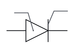
In the diode symbol shown here, the bar end is the cathode (K) and the other end the anode (A). The diode is forward biased when its anode is more positive than its cathode, whichever way the symbol is drawn.Source 1Source 2Source 3
Symbol and what it is doing
Pick the voltage applied to each end and a model. The printed diode never changes; the highlight shows the bias and whether that model lets current through.
Zero bias. The applied potentials are equal, so this comparison shows no forward-bias difference. Under the ideal model, zero voltage drop alone does not determine a current.
Reverse bias. The applied anode-side potential is lower: this is a reverse-bias comparison. The ideal diode model blocks reverse current.
Reverse bias. The applied anode-side potential is lower: this is a reverse-bias comparison. The ideal diode model blocks reverse current.
Forward bias. The applied anode-side potential is higher: this is a forward-bias comparison. The ideal model permits anode-to-cathode current in the stated current-limited test; the applied values are not loaded diode voltages.
Forward bias. The applied anode-side potential is higher: this is a forward-bias comparison. The ideal model permits anode-to-cathode current in the stated current-limited test; the applied values are not loaded diode voltages.
Zero bias. The applied potentials are equal, so this comparison shows no forward-bias difference. Under the ideal model, zero voltage drop alone does not determine a current.
Reverse bias. The applied anode-side potential is lower: this is a reverse-bias comparison. The ideal diode model blocks reverse current.
Forward bias. The applied anode-side potential is higher: this is a forward-bias comparison. The ideal model permits anode-to-cathode current in the stated current-limited test; the applied values are not loaded diode voltages.
Forward bias. The applied anode-side potential is higher: this is a forward-bias comparison. The ideal model permits anode-to-cathode current in the stated current-limited test; the applied values are not loaded diode voltages.
Forward bias. The applied anode-side potential is higher: this is a forward-bias comparison. The ideal model permits anode-to-cathode current in the stated current-limited test; the applied values are not loaded diode voltages.
The cathode is a terminal name, not a permanently negative terminal. During forward conduction conventional current leaves it. A cathode can be at +5 V while the anode is more positive.
Zero bias. The applied potentials are equal, so this comparison shows no forward-bias difference. Under the ideal model, zero voltage drop alone does not determine a current.
Forward bias. The applied anode-side potential is higher: this is a forward-bias comparison. The ideal model permits anode-to-cathode current in the stated current-limited test; the applied values are not loaded diode voltages.
Reverse bias. The applied anode-side potential is lower: this is a reverse-bias comparison. The ideal diode model blocks reverse current.
Reverse bias. The applied anode-side potential is lower: this is a reverse-bias comparison. The ideal diode model blocks reverse current.
Reverse bias. The applied anode-side potential is lower: this is a reverse-bias comparison. The ideal diode model blocks reverse current.
Zero bias. The applied potentials are equal, so this comparison shows no forward-bias difference. Under the ideal model, zero voltage drop alone does not determine a current.
A diode is forward biased when its anode potential is higher than its cathode potential, and reverse biased when the cathode is higher. Page orientation does not decide bias; the current also depends on the model and connected circuit.
Zero bias, below the 0.7 V offset. The applied anode-side potential is less than 0.7 V above the cathode-side potential. It is below the offset-model comparison boundary, so this model does not permit forward conduction in the stated test.
Reverse bias, below the 0.7 V offset. The applied anode-side potential is less than 0.7 V above the cathode-side potential. It is below the offset-model comparison boundary, so this model does not permit forward conduction in the stated test.
Reverse bias, below the 0.7 V offset. The applied anode-side potential is less than 0.7 V above the cathode-side potential. It is below the offset-model comparison boundary, so this model does not permit forward conduction in the stated test.
Forward bias, above the 0.7 V offset. The applied anode-side potential exceeds the cathode-side potential by more than 0.7 V. It is above the offset-model comparison boundary; the connected circuit would determine the current.
Forward bias, above the 0.7 V offset. The applied anode-side potential exceeds the cathode-side potential by more than 0.7 V. It is above the offset-model comparison boundary; the connected circuit would determine the current.
Zero bias, below the 0.7 V offset. The applied anode-side potential is less than 0.7 V above the cathode-side potential. It is below the offset-model comparison boundary, so this model does not permit forward conduction in the stated test.
Reverse bias, below the 0.7 V offset. The applied anode-side potential is less than 0.7 V above the cathode-side potential. It is below the offset-model comparison boundary, so this model does not permit forward conduction in the stated test.
Forward bias, above the 0.7 V offset. The applied anode-side potential exceeds the cathode-side potential by more than 0.7 V. It is above the offset-model comparison boundary; the connected circuit would determine the current.
Forward bias, above the 0.7 V offset. The applied anode-side potential exceeds the cathode-side potential by more than 0.7 V. It is above the offset-model comparison boundary; the connected circuit would determine the current.
Forward bias, above the 0.7 V offset. The applied anode-side potential exceeds the cathode-side potential by more than 0.7 V. It is above the offset-model comparison boundary; the connected circuit would determine the current.
The cathode is a terminal name, not a permanently negative terminal. During forward conduction conventional current leaves it. A cathode can be at +5 V while the anode is more positive.
Zero bias, below the 0.7 V offset. The applied anode-side potential is less than 0.7 V above the cathode-side potential. It is below the offset-model comparison boundary, so this model does not permit forward conduction in the stated test.
Forward bias, above the 0.7 V offset. The applied anode-side potential exceeds the cathode-side potential by more than 0.7 V. It is above the offset-model comparison boundary; the connected circuit would determine the current.
Reverse bias, below the 0.7 V offset. The applied anode-side potential is less than 0.7 V above the cathode-side potential. It is below the offset-model comparison boundary, so this model does not permit forward conduction in the stated test.
Reverse bias, below the 0.7 V offset. The applied anode-side potential is less than 0.7 V above the cathode-side potential. It is below the offset-model comparison boundary, so this model does not permit forward conduction in the stated test.
Reverse bias, below the 0.7 V offset. The applied anode-side potential is less than 0.7 V above the cathode-side potential. It is below the offset-model comparison boundary, so this model does not permit forward conduction in the stated test.
Zero bias, below the 0.7 V offset. The applied anode-side potential is less than 0.7 V above the cathode-side potential. It is below the offset-model comparison boundary, so this model does not permit forward conduction in the stated test.
The 0.7 V offset model uses a fixed 0.7 V drop during forward conduction and no forward conduction below that boundary. Here the controls compare applied source potentials, not solved diode terminal voltages.
Parts of the drawing
-
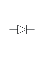
0°
-
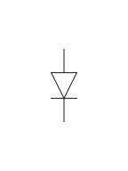
90°
-
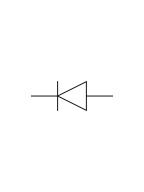
180°
-
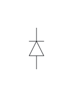
270°
-
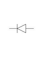
Mirrored
Rotating or mirroring a whole symbol, with its terminal identities and connections preserved, does not change the component. The terminal labels move with the drawing.Source 6
Variants
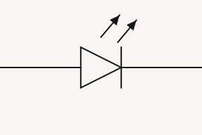
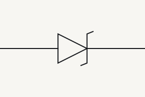
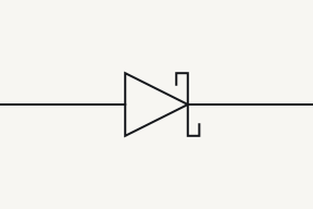
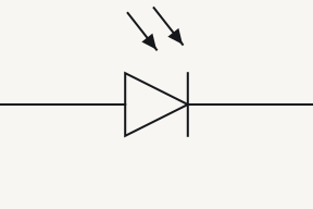
Every diode variant here keeps the triangle and bar and adds one mark: arrows leaving the body for an LED, arrows arriving for a photodiode, bent bar ends for a Zener and hooked bar ends for a Schottky. With no added mark it is a generic diode.Source 1Source 3
- AK
LED (light-emitting diode)
Two arrows leaving the diode body mark a light-emitting diode.Source 1
- AK
Zener diode
Bent ends on the cathode bar mark a Zener diode, a diode meant to be used in reverse breakdown.Source 1Source 3
- AK
Schottky diode
Hooked ends on the cathode bar mark a Schottky diode.Source 1Source 3
- AK
Photodiode
Two arrows arriving at the diode body mark a photodiode.Source 1
Often confused with
-
-
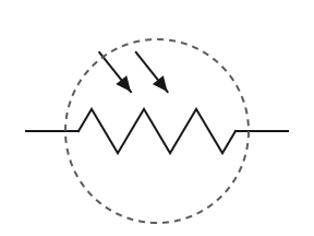
Light-dependent resistor
A resistor body
-
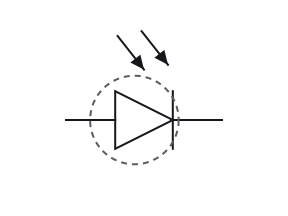
Photodiode
A diode's triangle and bar
An LDR and a photodiode both have arrows arriving at the body, so the body decides: a resistor body for an LDR, a diode's triangle and bar for a photodiode.Source 1Source 7
-
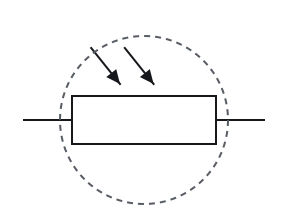
Light-dependent resistor
A resistor body
-
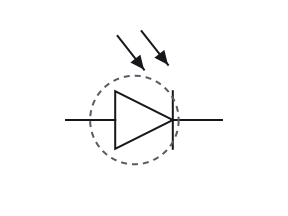
Photodiode
A diode's triangle and bar
An LDR and a photodiode both have arrows arriving at the body, so the body decides: a resistor body for an LDR, a diode's triangle and bar for a photodiode.Source 1Source 7
Fig. 4 — Light-dependent resistor and photodiode, the mark that tells them apart ringedLight-dependent resistor and photodiode, the mark that tells them apart ringed -
On the part
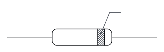
Where you meet it
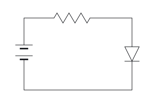
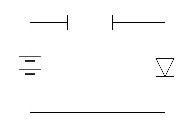
Notes
A diode passes current far more easily one way
A diode conducts much more readily in its forward direction than in its reverse direction. Real devices also have leakage and reverse breakdown, which this page's simplified models omit.Source 2Source 3 Its two ends are the anode and the cathode, and the overlay on this sheet compares their potentials under two named models. The transistor sheet sets the diode’s triangle beside the transistor and MOSFET arrows.
An LED may carry DS rather than D
In the IPC reference-designator list cited here, BT is a battery, CB a circuit breaker, DS a lamp, display or light-emitting diode, and RT a thermistor. Other naming systems use other letters.Source 4 So the letter beside an LED depends on the reference-designator list the drawing follows; its drawing is a diode’s triangle and bar either way.
Check your reading
More questions on the practice pagePick an answer to see the reason.
Answer key
- 1
The bar end
- 2
Forward biased: the anode is more positive than the cathode
AKapplied+12 Vapplied+5 V - 3
The anode's voltage compared with the cathode's
- 4
A light-emitting diode (LED)
- 5
Reverse biased, so it blocks
AKapplied0 Vapplied+5 V
Questions
Print and files
Printable symbol sheetPrintable symbol sheet More worksheets
-
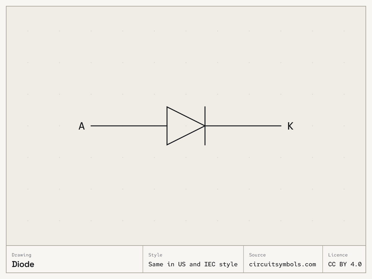 Same in US and IEC style PNG, 1200 × 900 SVG, line art
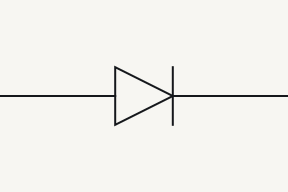
Variants as SVG line art: LED (light-emitting diode), Zener diode, Schottky diode, Photodiode
Sources
12 sources, numbered as cited
- Lessons In Electric Circuits, Vol. V — §9, Circuit Schematic Symbols (pp. 130–139)
- Diodes — terminal polarity, ideal and offset models (pp. 1–2, 7–10)
- ModEL — PN Junctions and Diodes, §§2.3–2.7 (bias and diode variants)
- Design to Manufacturing Standards — Reference Designators (slide 33)
- ModEL — Components and Symbols, §3.16 (diodes, p. 29)
- Electrical Schematics, §§1.3.1–1.3.5 — nodes, crossings, references and congruent drawings
- DC Electrical Circuit Analysis — resistive devices and schematic ground symbols (pp. 53, 59–64)
- Lessons In Electric Circuits, Vol. III — §3.1, diode representations (Figure 3.5, p. 100)
- Small-signal diode datasheet — forward-voltage graphs (p. 2)
- ModEL — Semiconductor Logic Gates, §2.1 (schematic versus package pinout, p. 8)
- ModEL — Electromechanical Relays, §§3.2–3.3 and §5.1 (normal and present contact status)
- ModEL — Components and Symbols, §3.17 (LED symbol, p. 31)